How Semiconductor Packaging Facilities Differ from Semiconductor Fabs?
India’s semiconductor ambitions are making headlines, with new investments in both chip fabrication (fabs) and advanced packaging. Yet, many factory owners and industry leaders still confuse these two critical parts of the chip supply chain.
Understanding their differences is essential for anyone planning to invest, partner, or expand in this sector.
What Happens Inside a Semiconductor Fab?
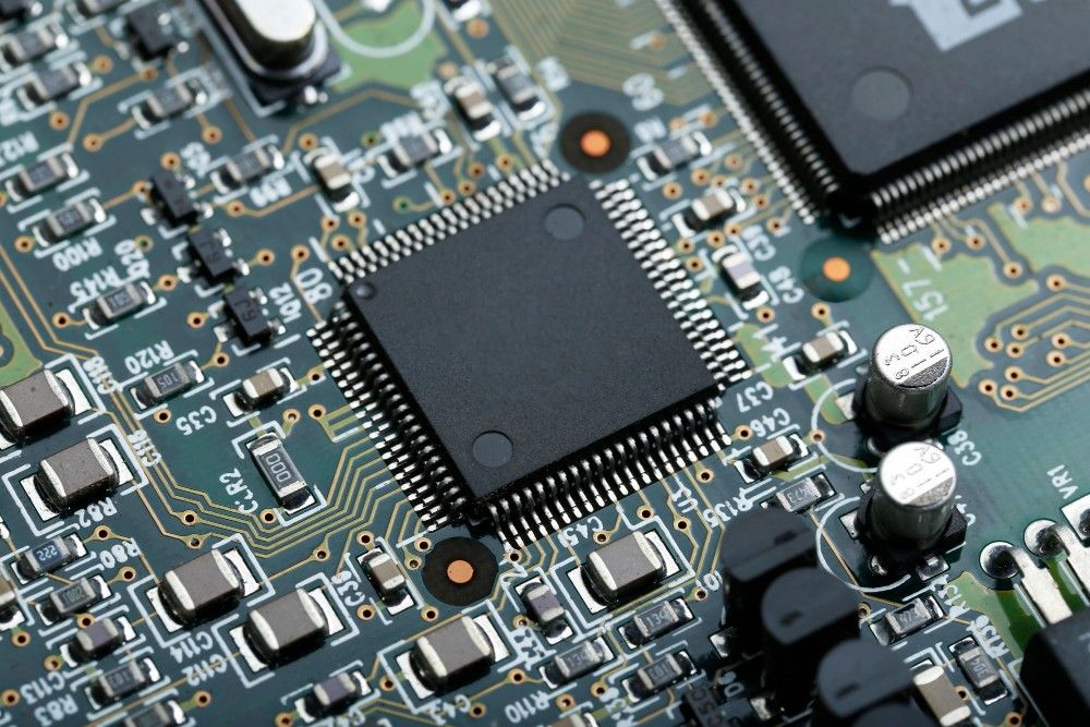
A semiconductor fab, or fabrication plant, is where the actual silicon chips are created. This process starts with pure silicon wafers and involves hundreds of steps like, photolithography, etching, doping, and deposition to build intricate circuits at the nanometer scale.
Fabs are among the most capital-intensive and technologically advanced facilities in the world. They require ultra-clean environments (cleanrooms), advanced process equipment, and highly skilled engineers. Even a speck of dust can ruin a batch of chips, so fabs maintain strict controls on air quality, temperature, and humidity.
In India, the push for domestic fabs is driven by the need for self-reliance in electronics and to reduce dependence on imports.
However, building a fab is a multi-billion-dollar, multi-year effort, with high barriers to entry and long payback periods.
What Is the Role of a Semiconductor Packaging Facility?
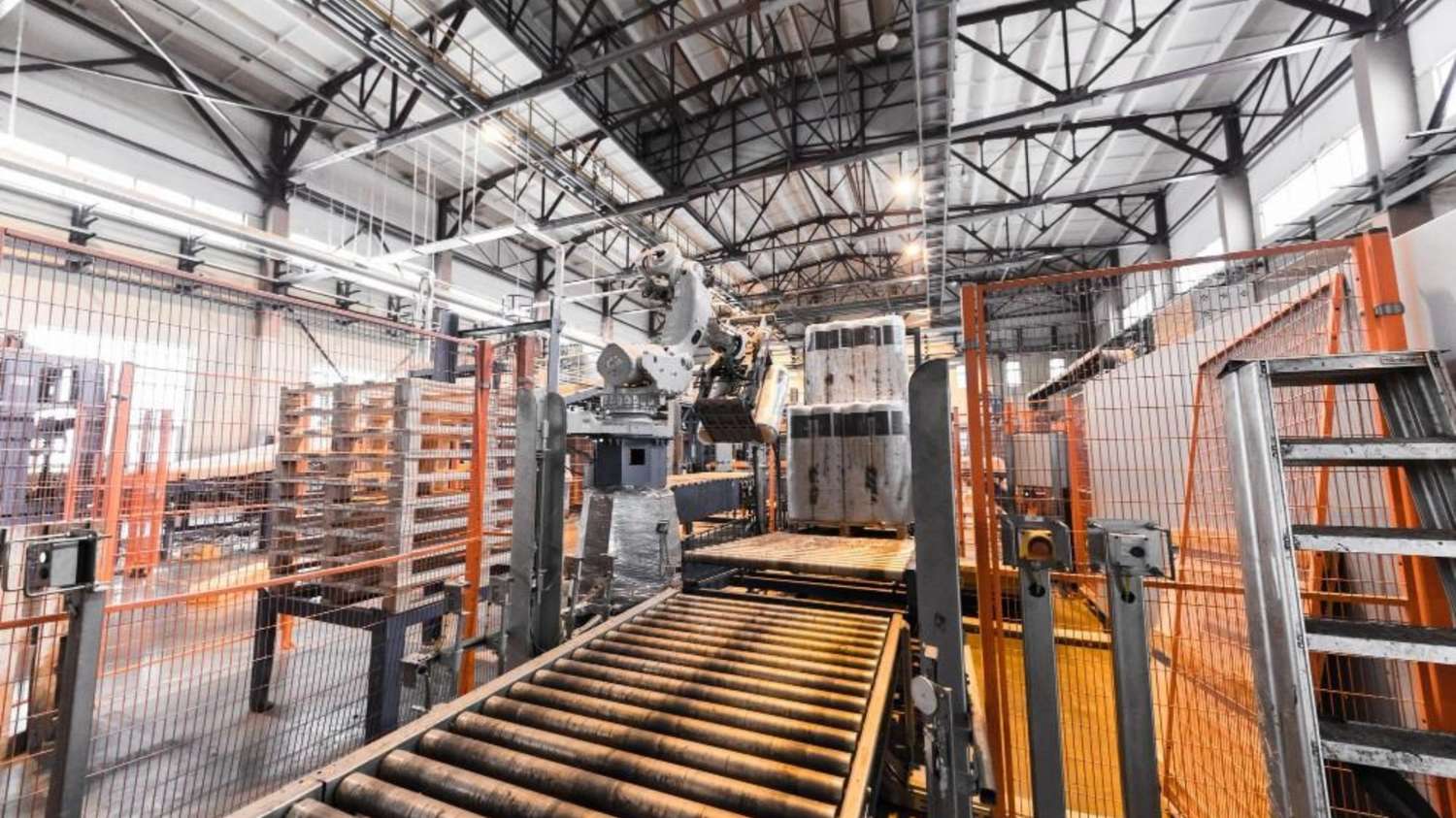
Once chips are manufactured in a fab, they are still fragile and unusable in their raw form. This is where packaging facilities come in. Packaging is the process of enclosing the chip in a protective case, connecting it to external pins or pads, and ensuring it can be safely integrated into electronic devices.
Packaging facilities focus on assembly, testing, and quality assurance. They use techniques like wire bonding, flip-chip, and advanced 3D packaging to connect chips to substrates. The goal is to protect the chip, manage heat, and enable reliable electrical connections.
Unlike fabs, packaging plants are less capital-intensive and can be set up more quickly. They play a crucial role in adding value, improving chip performance, and supporting the final stages of the electronics supply chain.
How Do Infrastructure and Facility Requirements Differ?
Fabs demand extremely high levels of cleanliness, advanced process gases, and massive power and water supplies. They often require custom-built cleanrooms with ISO Class 1–5 standards, specialized waste treatment, and 24/7 operations.
Packaging facilities, while still requiring clean environments, operate at less stringent standards (typically ISO Class 7–8). Their focus is more on precision assembly, automated handling, and testing equipment. Power and water needs are lower, and the risk profile is different—packaging plants are less vulnerable to contamination but must manage electrostatic discharge and mechanical stress.
For Indian investors, this means packaging facilities are more accessible as a first step into the semiconductor ecosystem, while fabs require deeper pockets and longer-term commitment.
What Are the Latest Trends in Packaging and Fabs?
Globally, the line between fabs and packaging is blurring with the rise of advanced packaging technologies. Innovations like chiplets, 2.5D/3D integration, and system-in-package (SiP) are making packaging a hotbed of R&D and value creation.
In India, recent announcements highlight a focus on both areas. New packaging plants are being set up in Gujarat and Telangana, aiming to serve global and domestic markets.
Meanwhile, the government’s semiconductor mission is attracting proposals for both fabs and OSAT (Outsourced Semiconductor Assembly and Test) units.
For factory owners, this means opportunities exist not just in chip making, but in the entire value chain from materials and equipment to packaging and testing.
What Should Factory Owners and Investors Consider?
Capital and Skills: Fabs need massive investment and highly specialized talent. Packaging plants require less capital but still demand skilled technicians and engineers.
Supply Chain Integration: Both types of facilities benefit from proximity to suppliers, logistics hubs, and end-users. Packaging plants, in particular, can thrive near electronics manufacturing clusters.
Technology Partnerships: Collaborating with global leaders in equipment, materials, and process technology is essential for both fabs and packaging units.
Regulatory and Incentive Landscape: India’s government offers incentives for both fabs and packaging, but the application process and compliance requirements differ.
Choose the Right Path in Semiconductors
Understanding the difference between fabs and packaging facilities is key to making informed decisions in India’s fast-evolving semiconductor landscape.
Whether you’re planning a new facility or upgrading an existing one, aligning your strategy with your resources and market needs is crucial.
Connect with VMS Consultants for expert guidance in engineering, architecture, and project management for your next high-tech project.
Let’s build the future of Indian electronics.